2013 Workshop on Si/GaAs/GaN RF Device Modeling, Design & Fabrication
Time: October 22,2013
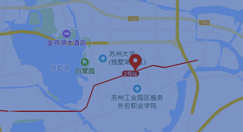
Venue: 106 Auditorium, National University of Singapore Suzhou Research Institute
Workshop Program
|
Time |
Topic |
Speaker |
|
13:00 – 13:05 |
Opening Address |
Dr.Yongxin GUO |
|
13:05 – 13:35 |
Breakthroughs of China Semi- conductor |
Dr. Shining YANG |
|
13:35 – 14:05 |
Recent Progress of Gallium Nitride RF-devices |
Dr. Naiqian ZHANG |
|
14:05 – 14:35 |
Evolution of power device modelling and their applications in PA designs |
Dr. Hongxi XUE |
|
14:35 – 15:05 |
Advanced Modeling cum PA design validation for 3rd generation device technologies |
Prof. Fujiang LIN |
|
15:05 – 15:35 |
WIN GaAs Technology Introduction and PDK Environment Status |
Dr. Zhengguo LIN |
|
15:35 – 15:55 |
Coffee Break |
|
|
15:55 – 16:25 |
The difference between GaN and Silicon from material to application perspective |
Dr. Dajie ZENG |
|
16:25 – 16:55 |
RF device modeling in RFIC industry : practice and challenge |
Dr. Tianshu ZHOU |
|
16:55 – 17:25 |
Modelling and Design of Microwave and Millimeter-Wave GaAs/GaN Power Devices |
Dr. Zheng ZHONG |
|
17:25 – 17:55 |
FinFET Technology Challenges & EQ/Process Solutions |
Dr. Meisheng ZHOU |
|
17:55 – 18:00 |
Closing Remarks |
Prof. Guoqin XU |
Workshop registration or other further information can be found here:
NUSRI workshop registration form
2013 workshop program - NUSRI - CAMD_v4
Contact: Mr.Zhao 15850104931 or Mr.Pan 15050870666


