Perovskite nanocrystal scintillators for X-ray imaging
On 27 Aug 2018, a team led by Professor Liu Xiaogang, Senior Investigator and Director of Centre for Functional Materials at NUSRI SZ, published their recent research findings in Nature. From the study, they developed a highly sensitive perovskite-based X-ray flat panel detector for imaging applications.
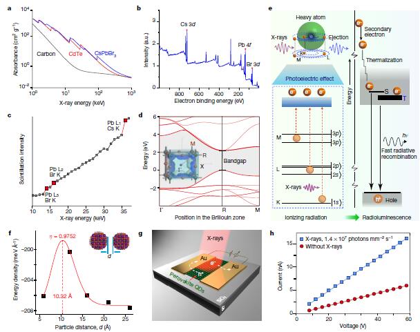
Since the 1890s, X-ray imaging technology has been widely used for many applications, including medical diagnostics, homeland security, national defence, advanced manufacturing, nuclear technology and environmental monitoring. Modern X-ray imaging uses scintillator materials as photodetectors to convert the high-energy X-rays into visible light. Most of these scintillator materials are made from expensive inorganic crystals, which are grown at high temperatures. Apart from the cost, these materials usually have a low radioluminescence yield (poor X-ray ionisation to light emission conversion efficiency).
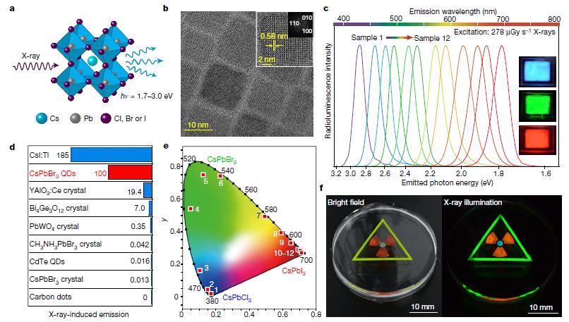
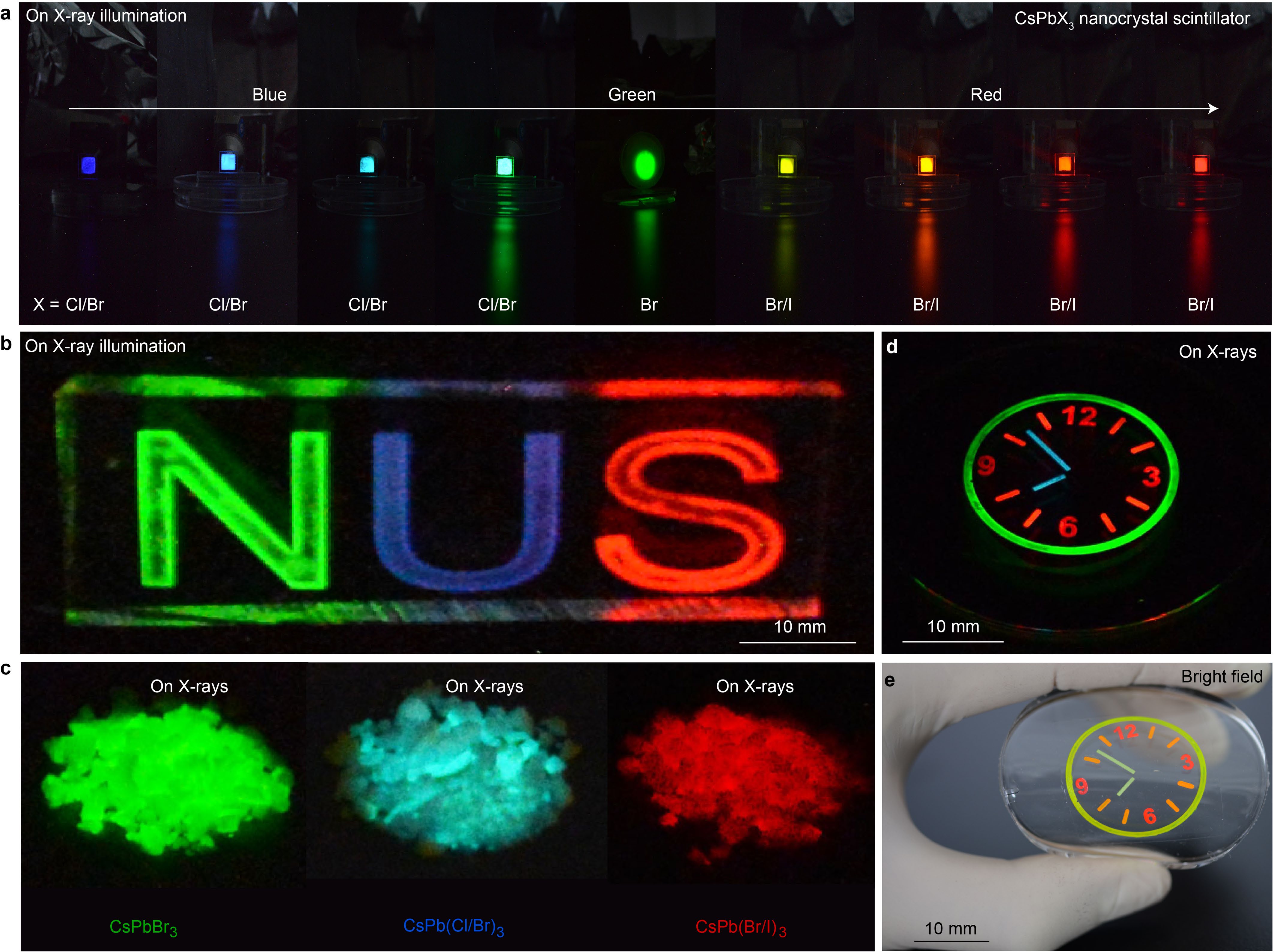
The team involving Professor Liu Xiaogang in collaboration with other local and international researchers, has discovered that lead halide perovskite nanocrystals are highly sensitive to X-ray irradiation and can detect small doses of X-ray photons, converting them into visible light. The colour of the light emission from these nanocrystals can be adjusted by varying the material composition of the perovskite nanocrystal. Conventional scintillators are usually produced using a solid-growth method at high temperatures. This makes it difficult to fabricate thin large uniform scintillator films. Unlike other scintillators made from inorganic crystals, these perovskite nanocrystals are solution processable (can be made with comparatively inexpensive processes) at a relatively low temperature. Using the nanocrystals, the researchers developed X-ray detectors with a detection limit of 13 nGyair s-1. This is about 400 times lower than the typical radiation dose used in medical diagnostics.
They are also highly sensitive to X-rays and easily detected using a camera. This means that they can potentially be developed as a convenient visualisation tool for X-ray radiography, in which the associated image can be directly recorded using low-cost, widely accessible digital cameras. This capability is not possible for conventional bulky scintillators, in which coherent scattering can occur and cause scintillation light loss.
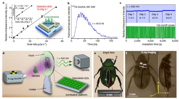
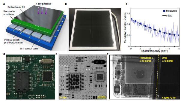
By incorporating these nanocrystal scintillators into commercial flat-panel X-ray imagers, the team has also demonstrated their potential for examining the internal structures of electronic circuit boards. Although X-rays are currently used in industry, perovskite nanocrystals can potentially offer a lower cost X-ray imaging technology with higher sensitivity.
Prof Liu said, “The discovery of perovskite nanocrystal scintillators has significant implications for many fields of research and could lead to new industrial applications. For example, low-cost, high-sensitivity X-ray imaging systems can potentially lower medical expenses and reduce the radiation risk to patients.”